
On June 4th, Dr. DAI Zhigao (First Author), appointed professor of CUG, Professor QIU Chengwei from the National University of Singapore (Corresponding Author), and Professor BAO Qiaoliang from Monash University (Corresponding Author) co-published a review paper entitled “Artificial Metaphotonics Born Naturally in Two Dimensions” in the top international chemistry journal Chemistry Review (Impact Factor: 54.301 in 2019; rank in chemistry journals: 1/172). The Engineering Research Center of NanoGeomaterials of Ministry of Education, School of Materials Science and Chemistry is the first author’s affiliation. Dr. HU Guangwei from National University of Singapore, OU Qingdong, postdoctoral fellow from Monash University, ZHANG Lei, researcher from Xi’an Jiaotong University, Professor XIA Fengnian from Yale University, and Professor Francisco J. Garcia-Vidal from the Autonomous University of Madrid are contributors to this paper.
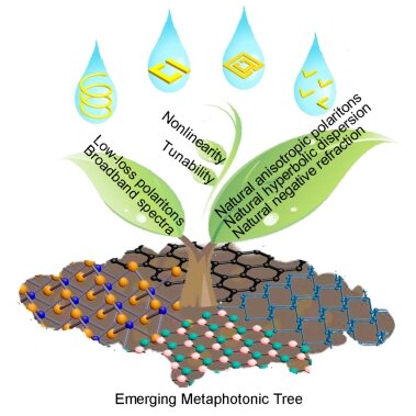
Figure 1. Artificial Metaphotonics Born Naturally in Two Dimensions
Two exciting scientific fields—layered two-dimensional (2D) materials and metaphotonics—overlap. Metaphotonics are artificial, engineered materials with broad application prospects, such as negative refraction index, lens and imaging, cloaks, optical perfect absorber and so on. Metamaterials naturally born in 2D materials that are 2D metamaterials or metasurfaces, have been exploited recently. In this review, we show that the concept of metamaterials naturally born in layered two-dimensional materials. 2D materials exhibit diverse optical properties, such as natural negative materials, natural hyperbolic materials, and natural anisotropic plasmonic materials. 2D materials possess natural meta-surface that are tunable and adjustable by micro-and nanofabrication. In addition, a combination of 2D materials with conventional metamaterials promises a variety of vibrant applications. The multi-functionality of 2D materials means that 2D materials-inspired metamaterials may enable the manufacturing of novel optical devices working in broad frequency ranges—from the visible to terahertz—with particularly low-loss, high speed, gated-tunability and miniaturized sizes. Metamaterials naturally born in 2D materials link fields of photonics, optoelectronics and plasmonics with metamaterials, and may provide insights to future innovations of 2D material-inspired meta-surface and metamaterials devices.
Metamaterials are artificial, engineered materials with reasonably designed compositions and arrangements of nanostructures. The metamaterial-based designs and demonstrations have broad application prospects, such as negative refraction index, lens and imaging, cloaks, optical perfect absorber and so on. Fabricating devices larger than a handful of unit-cell thick has been a constant challenge hampering metamaterials technology. Metamaterials also suffer from high resistive losses, narrow response range, and weak tunabilities. In recent years, the focus of metamaterial research has moved towards active and tunable metamaterials, in addition to simplifying structures while conserving many of their uncommon properties and functionalities.
Metamaterials naturally born in 2D materials that are 2D metamaterials or metasurfaces, have been exploited recently. These are much thinner than the working wavelength. In theory, the thinner thickness make layered 2D materials easier to engineer and less sensitive to absorption losses. By increasing the complexity of the internal composition and the collective coupling of “meta-atoms”, metasurfaces yield efficiencies comparable to bulk metamaterials.
Furthermore, by combining traditional metamaterials with 2D materials such as graphene, transition metal dichalcogenides, and black phosphor, optically and electrically tunable metasurfaces can be realized. Performances such as negative refraction, transmission, cloaking, have been anticipated through metasurfaces. With such progress we can expect the key point that they will play in photonics technology, for example, by providing tuneable functions for super-lenses, beam steerers and beam shapers.
This review will appeal broad communities, including physicists, material scientists, chemists, and device and optical engineers. The scope will cover basic structures, materials engineering, fundamental physics,andphotonic and optoelectronic devices. The existing results and promising future of natural metamaterials based on 2D materials will be of interest to researchers and experts who are new to the field.
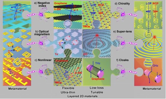
Figure 2. Artificial Metaphotonics Born Naturally in Two Dimensions
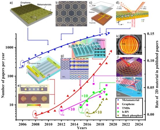
Figure3. Development history of Metamaterials and two-dimensional materials Inspire Each Other. The number of publications per year in the field of metaphotonics (blue line) and the rate of publications relevant to graphene (red line), TMDs (magenta line), hBN (green dots), and BP (dark yellow dots) between January 2006 and December 2019 (data from ISI Web of Knowledge, February 2020). Solid lines represent the exponential growth experienced in these areas. Dashed arrows depict the deliberate speculations of future trends.
Dr. DAI Zhigao received his Ph.D. degree (2015) in Condensed Matter Physics from Wuhan University. He was a lecturer and postdoctoral research fellow at the School of Printing and Packaging and theSchool of Physics and Technology respectively at Wuhan University until August 2019.From November 2016 to December 2018, he was awarded a scholarship under the International Postdoctoral Exchange Fellowship Program by the Office of China Postdoctoral Council as a postdoctoral research fellow at the Department of Materials Science and Engineering, Monash University. In September 2019, he joined the School of Materials Science and Chemistry, China University of Geosciences, as Appointed Professor. His research interests include plasmons, polaritons in van der Waals materials, and photonics and optoelectronic devices based on noble materials, 2D materials, and perovskites.
(from http://en.cug.edu.cn/info/1229/2432.htm )